:format(jpeg)/uploads/tedium112718.gif)
/uploads/tedium112718.gif)

Socket To Me
Why the processor socket, an important part of most desktop computers, lost its upgrade path as computers became smaller and more integrated.
Today’s GIF comes from a video of a guy talking about how to extract gold from old CPUs. Because really, why not?

Sponsored By 1440
News Without Motives. 1440 is the daily newsletter helping 2M+ Americans stay informed—it’s news without motives, edited to be unbiased as humanly possible. The team at 1440 scours over 100+ sources so you don't have to. Culture, science, sports, politics, business, and everything in between—in a five-minute read each morning, 100% free. Subscribe here.
“Dual in-line is a little larger than military-aerospace type packages. It is also a lot easier to work with. (Insert it by hand or by machine.) Its leads have dimensional tolerances to fit holes drilled to commercial standards. Use standard circuit boards. Flow solder it. In fact, handle it the way you would any discrete component.”
— A passage from a 1965 advertisement for dual in-line packaging, a format for installing integrated circuits that Fairchild Semiconductor had invented the year prior. The chip format, which quickly took over the industry, essentially connected to a circuit board using a lineup of two rows of connecting pins. (This is the kind of chip layout the average person might think of when you use the term “microchip.”) The packaging format, which has become less common as the computer industry has started to make smaller machines with more dense processing processing power, nonetheless was widely used for decades, most notably in the Motorola 68000, a 64-pin chip used in many video game consoles as well as a trio of important 1980s computers: The Apple Macintosh, Commodore Amiga, and Atari ST.
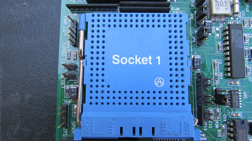
The Intel Socket 1, used for 486 chips. The socket has a zero insertion force (ZIF) mechanism. (KJanos1396/Wikimedia Commons)
Five interesting facts about processor sockets
1. The placement of the pins is often very specific. To ensure that a chip doesn’t get placed into a socket the wrong way, or to keep incompatible processors out of the sockets, the pin grid array (PGA) is often set up in an almost—but not quite—symmetrical way. This can be seen in one of the earliest CPU sockets to use a pin grid array, the Intel Socket 1, which dates to the days of the 486. The socket type has three perfectly square rows of pins on either side, minus one extra pin in the bottom-left corner, ensuring alignment is perfect. PGA was spearheaded by Intel but is still used heavily by AMD today.
2. You often don’t force chips into place. You know how, when you put an NES cartridge into the console, you have to press down to fully insert it—but not too hard, lest you bend the pins inside? (But you bend them anyway, because you were too aggressive?) Many replaceable chip adapters work like that, using something called a “zero insertion force” socket to hold things in place. With a ZIF chip socket, you basically get it lined up, and in many cases, use something to clamp it down into place—say, like a metal bar. The approach came into use with the goal of making it easier for end users to change out processors without a lot of hassle.
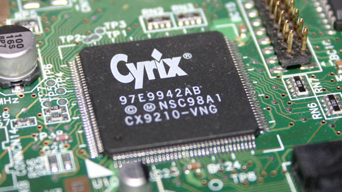
A Cyrix QFP chip. (Geoff Martin/Wikimedia Commons)
3. Some processors have pins that stick out to the side. Over the years, there have been lots of different kinds of chip layouts, some of which are more efficient in terms of the number of connections than others. One technique widely used in the early ’90s on many chips is the quad flat package (QFP), which attached to a piece of silicon using dozens or even hundreds of little pins that jutted out to either side. This technology, which can be soldered to a board by hand, eventually fell out of favor for top-tier CPUs, in part because newer technologies used space more efficiently, but you can still find examples around, such as this very inexpensive ARM chip.
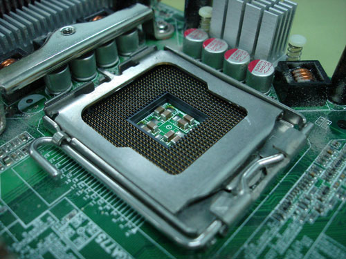
An Intel LGA 775 socket, which features pins on the motherboard itself, rather than on the chips. (stnc06/Flickr)
4. Major chip companies have been known to change up their techniques. When people think of processors, ten to one, they might be thinking about the pin grid used on many of Intel’s early chips, but it’s far from the only technique in use. For example, the Land Grid Array (LGA), used on many modern Intel chips and even some recent AMD chips, basically flips the model of the PGA chips, putting the contacts on the processor itself, but the pins on the motherboard. This allows for higher pin densities than PGAs, and when needed, a way to hold the chips into place using solder paste—a technique commonly used on laptops, where space is a luxury. Speaking of …
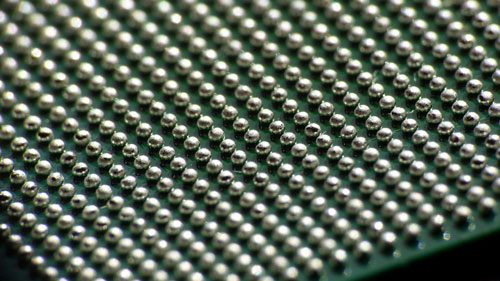
5. Many smartphone chips are held into place with tiny balls of solder. There obviously isn’t a ton of room for a processor on a socket in a smartphone or an ultra-thin laptop, so techniques for putting processors into place have evolved. One of these techniques is something called ball grid array, which involves the exact placement of balls of solder in a layout not dissimilar to that used in a pin grid array or a land grid array. Why solder? For one thing, it takes up less space than a mechanism that allows a device to be easily removed; for another, it’s more efficient, as the entire chip can be held down by balls of solder, an approach that allows for the shrinking of components, such as solid-state drives, to ever-smaller sizes. The downside for consumers, of course, is that it makes devices far less upgradeable, because it requires a level of precision that a machine can easily handle most humans can’t, and it’s way more complicated to desolder a chip than it is to solder one in, to the point where you’re better off buying a new phone than trying yourself. And, of course, sometimes things come loose, leading to things like the iPhone 6’s infamous “touch disease.”
“Today, a very significant part of the PC business has become a replacement business—selling second, third, or fourth generations of PCs to people and companies already in the games. And for the last two years, the buzzword has been upgradability.”
— A 1992 PC Magazine piece on the hot new trend in personal computers—upgradability. Computers could clearly handle upgrades before this, of course, but there seemed to be a real effort made towards computers with an upgrade path around this time, particularly on the CPU front, a move that later gave way to the growth in popularity of DIY computer builds. But as our technology evolved and became smaller, there was simply less room for this once-buzzworthy idea.
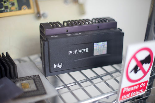
Intel’s slot-based Pentium II chip-on-a-cart. (James O’Gorman/Flickr)
That time Intel sold processors that looked like Sega Genesis cartridges
Fairchild Semiconductor, while never the most high-profile technology company, was notable for having a strong influence on the way that the computer industry moved forward in two specific ways: One, its company’s alumni were responsible for launching some of Silicon Valley’s most fundamental companies; and two, Fairchild also developed chip technology that came to define both the PC and video game industries.
A line, of course, can be drawn between dual in-line packaging and many of Intel’s socket-based pin-insertion formats on its processors. But the company, via its development of the Fairchild Channel F, had also come up with the first practical cartridge-based video game console, a design that relied on placing a printed circuit board inside of an edge connector. This edge connector approach, of course, also found use in a variety of mediums in computing, including with expansion ports in many desktop computing devices. The modern-day PCI Express slot, used to connect video cards to desktop computers, works much the same way.
And notably, the cartridge-style slot also gained currency as a way that many desktop machines of the late ’90s interacted with their processor. This was an idea used by Intel for its Pentium II and Pentium III processors, and came in two variants—the 242-contact Slot 1, and the 330-contact Slot 2, with the latter used on the higher-end Xeon chips, with larger bandwidth made available for its level 2 cache. These slots were designed to only work in one direction, and were intended to help Intel get around an issue it had faced in consistently combining its processor with a cache in its Socket 8 technology.
(To a degree, this approach makes sense; 8-bit and 16-bit video game consoles famously extended the power of the underlying console on some games by adding new chips directly on the cartridge, something seen most prominently with the Super FX chip.)
An Intel Slot 1, just waiting for an upright processor on a daughterboard. (Rainer Knäpper/Free Art License)
The decision to switch from the long-in-use socket approach to a slot was partly due to technical needs, but some wondered whether competitive issues also played a role. Some pointed to the fact that Socket 7, the previously used CPU installation scheme, was an open standard, while Slot 1 and Slot 2 were proprietary.
“It’s reasonable to infer that the new packaging for the Pentium II was [designed] to exclude competitors,” PC World editorial director Phil Lemmons told the Los Angeles Times in 1998.
This factor, among many, led to a Federal Trade Commission investigation, as concerns that Intel was trying to shut out AMD and Cyrix, among other competitors, were a major point of concern within the industry.
However, Intel’s move away from Socket 7 ended up backfiring, at least in part, due to two issues: One, the chip companies that relied on Socket 7 didn’t stop innovating using the old chip format, allowing them to come up with designs that were faster than Pentium CPUs, creating a competitive low end to the market, as well as an upgrade path for owners of older Pentium processors—which proved useful, as Intel’s own low-end Celeron chips failed to come up with the goods. That gave AMD in particular some breathing room as it struggled to keep up with its higher-profile competitor.
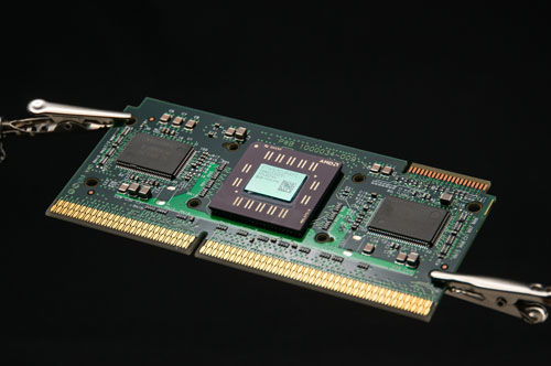
A first-generation AMD Athlon processor, shown without its casing. (Fritzchens Fritz/Flickr)
Intel’s efforts at gaining a competitive advantage over AMD would eventually make AMD a stronger company as it, too, embraced the slot, at least for a time. In 1999, AMD released a CPU line of its own called the Athlon, which used its own proprietary slot, called Slot A. While it wasn’t electrically the same as Intel’s own Slot 1, it had many physical similarities, including the same number of contacts and a very similar design. To avoid folks from accidentally shoving a Pentium II into the slot and frying their motherboard, the connector was flipped backward. The idea was clever—it made it possible for computer manufacturers already using the 242-contact edge connector to use that same connector, but on an AMD processor.
It was a somewhat confusing move, considering AMD initially fought against the slot tooth and nail. But it gave the company a path forward as a processor maker outside of Intel’s direct shadow, and soon it began creating its own sockets—along with lines of processors that stood out on their own, away from their long conflict with Intel.
“Despite kicking and screaming when Intel introduced its proprietary Slot 1, AMD eventually executed an about-face and bred its own version of the slot,” Maximum PC noted in a 2000 guide to processor sockets. “Why? Because AMD knew that to increase clock frequencies, take advantage of plentiful generic SRA, and keep its packaging reliable, it needed to move to a slotted system. With Slot A, AMD achieved those goals.”
The magazine noted that there were genuine issues with slotted processors, which probably makes sense if you’ve ever improperly put a Sega Genesis cartridge into the console. “Too often, slot 1 systems have failed to boot because the processor popped out during shipping,” the magazine noted. But the other issue was more fundamental: The drumbeat of technology was making the main reason for the slot’s existence, the desire to combine processor and cache onto a single plate of silicon, was made unnecessary thanks to the addition of L2 cache directly on the CPU die, allowing its Socket 370 to supersede it during the lifetime of the Pentium III.
While the processor slot only lived for a few short years, it did have a little bit of an afterlife thanks to an aftermarket device called the “Slotket,” which essentially was an aftermarket converter that placed a Socket 370 chip caddy to fit onto a daughterboard that fit inside a Slot 1.
Good luck finding one today, but it nonetheless highlights something useful about these slots and sockets—there was always an upgrade path, even if it was confusing.
It’s weird to think that, a quarter-century ago, our CPUs looked like video game cartridges, a move that weirdly feels like a bad memory today, in an era when computers take up less and less room, where many highly-integrated modern computers would never allow a CPU to take up anywhere near that much space.
But what’s great about those slotted chips is that, for all their faults, they could be removed and replaced by an end user.
Our move towards highly integrated, ever-smaller devices is, of course, a double-edged sword. On the one hand, moving to technologies that solder chips directly onto the board has been a real kick in the pants for speed and size. On the other hand, as chip sizes shrink as new techniques get used, the upgrade paths that we once had, both on mobile and in some desktop forms, become less clear.
The rise of the mini PC, as highlighted by the Intel NUC and the Mac Mini, has made it so that people are much more likely to replace an entire machine rather than go through the trouble of upgrading a processor, as an example.
I mean, that’s what people already do with smartphones.
This high level of integration means that our computers need to do the job a little bit longer, because once we buy ’em, we’re stuck with them a few years, and once you buy it, it’s what you own. Not even the RAM chips are easy to replace in many models. It’s a dead end, one that left a formerly buzzy idea—upgradability—on the cutting room floor.
More than a decade ago, YouTuber Dave Hakkens came up with a clever concept that effectively brought the modularity concept of desktop computers to the world of smartphones. PhoneBloks, as he called it, was a hugely inspiring kick in the pants for tech at the time it was announced, but after some missteps in the form of Google’s shuttered Project Ara, the idea had lost buzz and momentum as it seemed that the world had decided to go another direction entirely. In a retrospective from about four years ago, Hakkens remained optimistic, but the idea (when it has emerged) has largely leaned on the idea of repairability, not upgradeability.
Still, it’s hard not to watch the clip and feel an immense sense of disappointment that this big idea couldn’t keep up with the demands of ever-shrinking components. Hakkens’ instinct is right, but the hard part is that there’s no money, or at least not as much money, to be found in upgradeable components, e-waste be damned.
All that said, one company in the laptop market is helping to give postmarket upgraders some hope. That company, Framework, has released strategies to replace RAM, storage, batteries, even mainboards. The company uses ball-grid array chips, so the CPU won’t leave the board, but you can take it out, replace it with a new one, and even reuse the old one.
The processor socket, for all its complexities and technical quirks, represented a step in the favor of the consumer, even if just those technically minded enough to know how to upgrade a CPU on a motherboard or to know the difference between a pin grid array and a ball grid array.
Now, if we could only shrink our upgradability as fast as our processors.
--
Find this one an fascinating read? Share it with a pal!
Also, be sure to give our quick-hit newsletter Lesser Tedium a look—and get a two-minute look at one of the many elements in Tedium’s deep archives.
Is now the time to upgrade your news diet? Our sponsor 1440 can help.
/uploads/ernie_crop.jpg)